NCP1607
http://onsemi.com
18
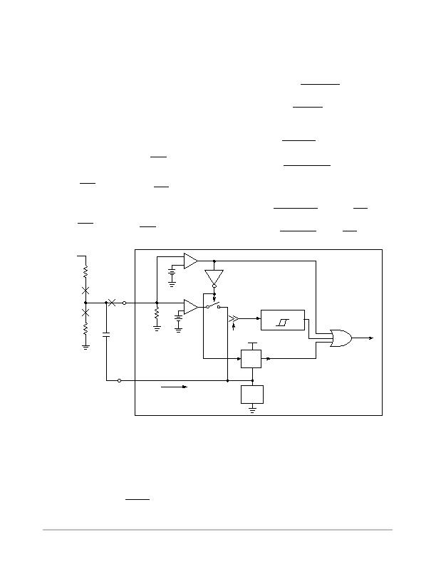
UVP and OVP protect the system from low bulk voltages
and rapid operating point changes respectively, while the
FPP protects the system against floating feedback pin
conditions. If FPP is not implemented and a manufacturing
error causes the feedback pin to float, then the feedback
voltage is dependent on the coupling within the system and
the surrounding environment. The coupled feedback
voltage may be within the regulation limits (i.e. above the
UVP threshold, but below V
REF
) and cause the controller
to deliver excessive power. The result is that the output
voltage rises until a component fails due to the voltage
stress.
The tradeoff for including FPP is that the value of R
FB
causes an error in the output voltage. The output voltage
including the error caused by R
FB
(V
OUT
) is calculated
using Equation 16:
V
OUT
+ V
OUT
) R
OUT1
@
V
REF
R
FB
(eq. 16)
Using the values from the OVP calculation, the output
voltage including the error caused by R
FB
is equal to:
V
OUT
+ 400 ) 4 M @
2.5
4.7 M
+ 402 V
The error caused by R
FB
is compensated by adjusting
R
OUT2
. The parallel combination of R
FB
and R
OUT2
form
an equivalent resistor R
EQ
that is calculated using
Equation 17.
R
EQ
+ R
OUT1
@
V
REF
V
OUT
* V
REF
(eq. 17)
R
EQ
+ 4 M @
2.5
400 * 2.5
+ 25.16 kW
R
EQ
is used to calculate R
OUT2
.
R
OUT2
+
R
EQ
@ R
FB
R
FB
* R
EQ
(eq. 18)
R
OUT2
+
25.16 k @ 4.7 M
4.7 M * 25.16 k
+ 25.29 kW
The compensated output voltage is calculated using
Equation 19.
V
OUT
+ V
REF
@
R
OUT1
) R
OUT2
R
) R
OUT1
@
V
REF
R
(eq. 19)
V
OUT
+ 2.5 @
4 M) 25.29 k
25.29 k
) 4 M@
2.5
4.7 M
+ 400 V
Control
E/A
FB
UVP
Static OVP
Fault
Dynamic OVP
Enable
Condition 2
Condition 1
Condition 3
Figure 37. Open Feedback Loop Protection
+
-
+
+
-
+
R
FB
C
COMP
V
CONTROL
I
CONTROL
I
CONTROL
R
OUT2
R
OUT1
V
OUT
V
EAH
Clamp
V
DD
V
EAL
Clamp
Measure
Static OVP is triggered
when clamp is activated
(Enable EA)
I
CONTROL
> I
ovp
V
REF
V
UVP
Overcurrent Protection (OCP)
A dedicated pin on the NCP1607 senses the peak current
and limits the driver on time if this current exceeds
V
CS(limit)
. This level is 0.5 V (typical). Therefore, the
maximum peak current can be adjusted by changing R
SENSE
according to:
I
peak
+
V
CS(limit)
R
S
(eq. 20)
An internal LEB filter (Figure 38) reduces the likelihood
of switching noise falsely triggering the OCP limit. This
filter blanks out the first 250 ns (typical) of the current
sense signal. If additional filtering is necessary, a small RC
filter can be added between R
SENSE
and the CS pin.
发布紧急采购,3分钟左右您将得到回复。
相关PDF资料
NCP1611BDR2G
IC PFC CTLR HE ENHANCED 8-SOIC
NCP1651DR2G
IC PFC CONTROLLER CCM/DCM 16SOIC
NCP1654BD133R2G
IC PFC CCM 133KHZ 8-SOIC
NCP1927DR2G
IC CTLR PFC/FLYBACK 16-SOIC
NCP380HMU21AATBG
IC CURRENT LIMIT SWITCH 6-UDFN
NCT1008DMT3R2G
TMP DIO MON/SMBUS 4CH 8WDFN
NCT210RQR2G
IC TEMP SENSOR LOC/REM 16QSOP
NCT214MT3R2G
IC TEMP SENSOR LOC/REM 10WDFN
相关代理商/技术参数
NCP1607BOOSTGEVB
功能描述:BOARD EVAL NCP1607 100W BOOST RoHS:是 类别:编程器,开发系统 >> 评估演示板和套件 系列:* 标准包装:1 系列:PCI Express® (PCIe) 主要目的:接口,收发器,PCI Express 嵌入式:- 已用 IC / 零件:DS80PCI800 主要属性:- 次要属性:- 已供物品:板
NCP1608BDR2G
功能描述:功率因数校正 IC COST EFFECT PWR FACT CONT RoHS:否 制造商:Fairchild Semiconductor 开关频率:300 KHz 最大功率耗散: 最大工作温度:+ 125 C 安装风格:SMD/SMT 封装 / 箱体:SOIC-8 封装:Reel
NCP1608BOOSTGEVB
功能描述:电源管理IC开发工具 NCP1608 100 W BOOST EVB PWR SPY
RoHS:否 制造商:Maxim Integrated 产品:Evaluation Kits 类型:Battery Management 工具用于评估:MAX17710GB 输入电压: 输出电压:1.8 V
NCP1611ADR2G
功能描述:功率因数校正 IC NCP1611A ENHANCED PFC
RoHS:否 制造商:Fairchild Semiconductor 开关频率:300 KHz 最大功率耗散: 最大工作温度:+ 125 C 安装风格:SMD/SMT 封装 / 箱体:SOIC-8 封装:Reel
NCP1611BDR2G
功能描述:功率因数校正 IC NCP1611A ENHANCED PFC RoHS:否 制造商:Fairchild Semiconductor 开关频率:300 KHz 最大功率耗散: 最大工作温度:+ 125 C 安装风格:SMD/SMT 封装 / 箱体:SOIC-8 封装:Reel
NCP1611GEVB
制造商:ON Semiconductor 功能描述:PG - ACDC CONVERSION - Bulk 制造商:ON Semiconductor 功能描述:EVAL BOARD, NCP1611, POWER FACTOR CORRECTION; Silicon Manufacturer:On Semiconductor; Silicon Core Number:NCP1611; Kit Application Type:Power Management; Application Sub Type:Power Factor Correction (PFC) ;RoHS Compliant: Yes
NCP1612ADR2G
功能描述:功率因数校正 IC
RoHS:否 制造商:Fairchild Semiconductor 开关频率:300 KHz 最大功率耗散: 最大工作温度:+ 125 C 安装风格:SMD/SMT 封装 / 箱体:SOIC-8 封装:Reel
NCP1612BDR2G
制造商:ON Semiconductor 功能描述:ENHANCED HIGH-EFFICIENCY - Tape and Reel
